AKTU B.Tech. 3rd Year V Semester KEC-501 Integrated Circuit Class Notes:
Unit-IV AKTU IC Syllabus:
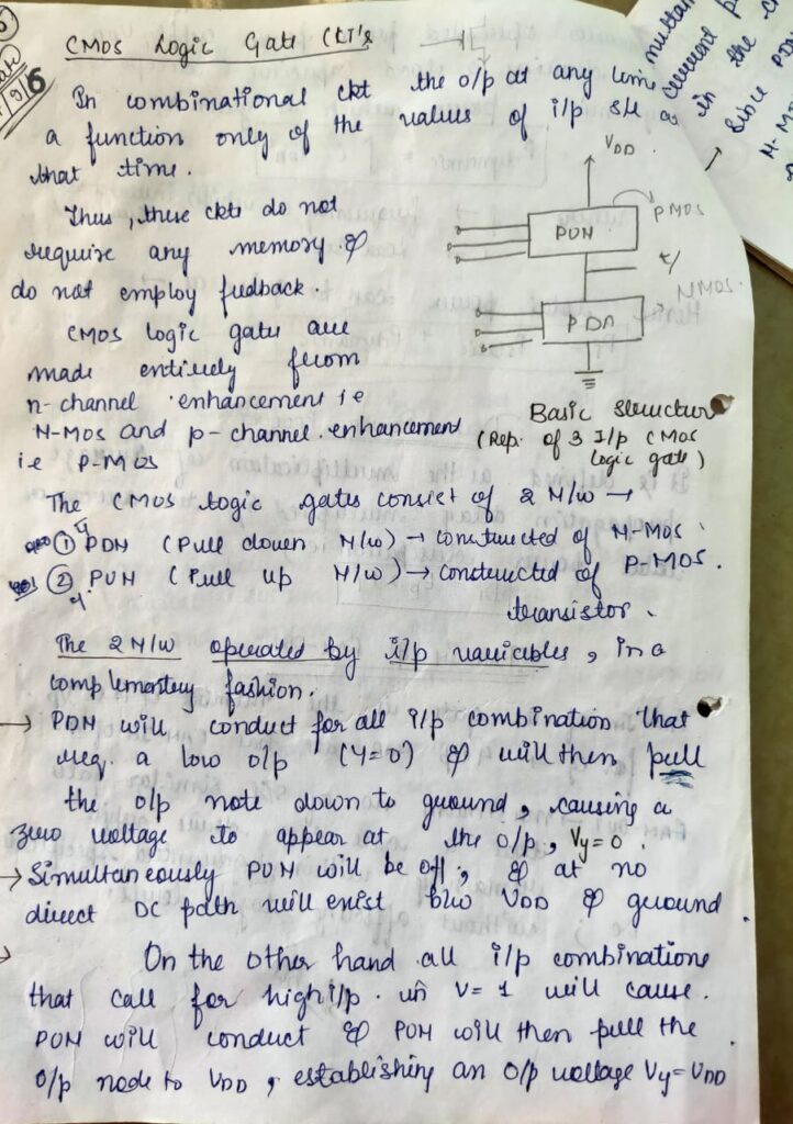
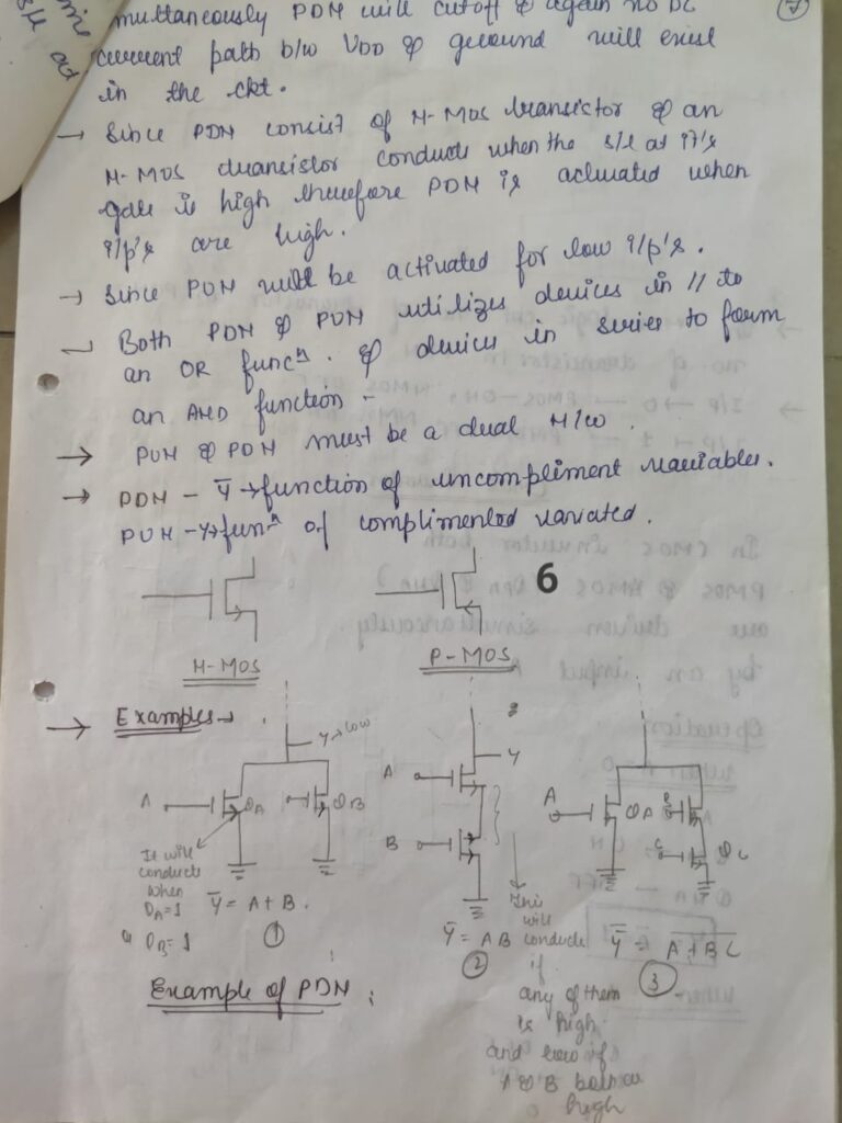
Digital Integrated Circuit Design: An overview, CMOS logic gate circuits basic structure, CMOS realization of inverters, AND, OR, NAND and NOR gates, Latches and Flip flops: the latch, CMOS implementation of SR flip-flops, a simpler CMOS implementation of the clocked SR flip-flop, CMOS implementation of J-K flip-flops, D flip- flop circuits.
_____________________________________________________________________________________

Multiple Choice based questions of IC Sessional-1
- Which of these is incorrect for an operational amplifier?
a) It has a high voltage gain
b) It is a direct-coupled amplifier
c) It is only useful for amplifying AC signals
d) It was originally designed to perform mathematical operations - In an ideal op-amp, which is not true?
a) Open-loop voltage gain is infinite
b) Input resistance is infinite
c) Slew rate is infinite
d) CMRR is zero - In negative logic convention, the Boolean Logic [1] is equivalent to:
a) +VDD
b) 0 V
c) -VDD
d) None of the mentioned - In positive logic convention, the true state is represented as:
a) 1
b) 0
c) -1
d) -0
- In CMOS logic circuit the n-MOS transistor acts as:
a) Load
b) Pull up network
c) Pull down network
d) Not used in CMOS circuits - In CMOS logic circuit the p-MOS transistor acts as:
a) Pull down network
b) Pull up network
c) Load
d) Short to ground - In CMOS logic circuit, the switching operation occurs because:
a) Both n-MOSFET and p-MOSFET turns OFF simultaneously for input ‘0’ and turns ON simultaneously for input ‘1’
b) Both n-MOSFET and p-MOSFET turns ON simultaneously for input ‘0’ and turns OFF simultaneously for input ‘1’
c) N-MOSFET transistor turns ON, and p-MOSFET transistor turns OFF for input ‘1’ and N-MOS transistor turns OFF, and p-MOS transistor turns ON for input ‘0’
d) None of the mentioned - When both nMOS and pMOS transistors of CMOS logic design are in OFF condition, the output is:
a) 1 or Vdd or HIGH state
b) 0 or ground or LOW state
c) High impedance or floating(Z)
d) None of the mentioned - When both nMOS and pMOS transistors of CMOS logic gates are ON, the output is:
a) 1 or Vdd or HIGH state
b) 0 or ground or LOW state
c) Crowbarred or Contention(X)
d) None of the mentioned - The full form of CMOS is ____________
a) Capacitive metal oxide semiconductor
b) Capacitive metallic oxide semiconductor
c) Complementary metal oxide semiconductor
d) Complemented metal oxide semiconductor - CMOS is also sometimes referred to as ____________
a) Capacitive metal oxide semiconductor
b) Capacitive symmetry metal oxide semiconductor
c) Complementary symmetry metal oxide semiconductor
d) Complemented symmetry metal oxide semiconductor - CMOS technology is used in ____________
a) Inverter
b) Microprocessor
c) Digital logic
d) Both microprocessor and digital logic - Two important characteristics of CMOS devices are ____________
a) High noise immunity
b) Low static power consumption
c) High resistivity
d) Both high noise immunity and low static power consumption - CMOS behaves as a/an ____________
a) Adder
b) Subtractor
c) Inverter
d) Comparator - An important characteristic of a CMOS circuit is the ____________
a) Noise immunity
b) Duality
c) Symmetricity
d) Noise Margin - CMOS logic dissipates _______ power than NMOS logic circuits.
a) More
b) Less
c) Equal
d) Very High - Semiconductors are made of ____________
a) Ge and Si
b) Si and Pb
c) Ge and Pb
d) Pb and Au - The truth table for an S-R flip-flop has how many VALID entries?
a) 1
b) 2
c) 3
d) 4 - When both inputs of a J-K flip-flop cycle 1, the output will ___________
a) Be invalid
b) Change
c) Not change
d) Toggle - A basic S-R flip-flop can be constructed by cross-coupling of which basic logic gates?
a) AND or OR gates
b) XOR or XNOR gates
c) NOR or NAND gates
d) AND or NOR gates - The logic circuits whose outputs at any instant of time depends only on the present input but also on the past outputs are called (CO4R)
a) Combinational circuits
b) Sequential circuits
c) Latches
d) Flip-flops - The basic latch consists of ___________
a) Two inverters
b) Two comparators
c) Two amplifiers
d) Two adders - In S-R flip-flop, if Q = 0 the output is said to be ___________
a) Set
b) Reset
c) Previous state
d) Current state
- The transparent flip-flop is also called a) D FF
b) SR FF c) Master-Slave JK FF
d) T FF
Download Answers and your Marks:
B.Tech. 3rd Year V Semester ECE Scheme Download
0 Comments